Tuesday, June 14, 2011

Lab 10 - AC Signals #1

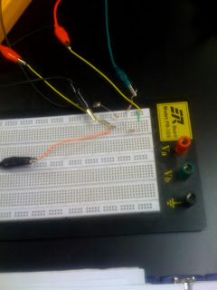
In this lab, we investigated AC signals and the corresponding phase effects on circuit elements.  This was achieved by hooking up an AC signal from a function generator into a simple RC circuit and then analyzing the results using an oscilloscope and multimeter.  The time difference between the signals was determined on the oscilloscope which was then used to determine the phase difference. 

Unfortunately no picture is available.


Data:
AC Signal3 V peak to peak @ 2 kHz
Anticipated V RMS2.12 V
Measured V RMS2.0 V
Z C-j717 ohm
V C peak to peak2 V
Measured VC RMS.61 V
∆t between sign90 ms
phase θ 199.8 deg


This phase angle indicates that capacitor signal leads the resistor.

Wednesday, May 11, 2011

Lab 9 - Oscilloscope 101


This lab was an introduction to the oscilloscope which is a tool used to analyze time-varying signals.  The scope operates by deflecting an electron beam onto a special phosphor-coated screen which lights up when the beam hits it.  Controls allow you to vary the voltage and time scale so that the input signal can be displayed as desired.  In our case we used a function generator to generate the 4 different signals below which could then be analyzed.  The first 3 were known sinusoid and squarewave signals with/without DC offsetting and the final was an unknown mystery signal.  This mystery signal appeared as a modified squarewave with a slight decay at the peaks.

Ex 1:5 kHz 5V Sinusoid
Period200 microsec
Pk-Pk ampl10 V
Zero-Pk ampl5 V
RMS3.53 V
DMM readings:
VDC0 V
VAC3.3 V
Ex 2:5 kHz Sinusoid w 2.5 V DC Offset
DMM readings:
VDC2.51 V
VAC3.32 V
Ex 3:5 kHz Squarewave w 2.5 V DC Offset
DMM readings:
VDC2.51 V
VAC5.25 V

Calculated RMS3.34 V
Ex 4:Mystery signal
DC voltage2.5 V
Frequency100 Hz
Pk-Pk Amp.4 V

Thursday, April 28, 2011

Lab 8 - Operational Amplifiers I


In this lab, we took a look at op amps by applying them to a real world scenario.  The idea was that in the real world, different sections of your circuit may require different signal voltages/currents.  In order to provide the correct signal to these sections, you have to pass them through an intermediate conditioning circuit, and op amps are an excellent way to produce the conditioning needed.  Our problem involved a conditioning circuit where the input needed to be 0 to 1V while the output need to be 0 to -10V.  So we created a voltage divider to provide the 0 to 1V input and then set up an op amp(LM741) as an inverting amplifier to get the 0 to -10V output.  The calculated values for the input and feedback resistors needed to produce a gain of -10 were Ri=1kohm and Rf=10kohm.  We used a variable resistor in our voltage divider to vary the input voltage at .25V increments from 0 to 1V and measured the output voltage at each reading.  The gains at each of these readings was then calculated and most came out to be right around -10. 

ComponentNominalMeasuredPower Rating
Ri1000 ohm990 ohm1/8 W
Rf10000 ohm9870 ohm1/8 W
Rx360 ohm354 ohm1/8 W
Ry68 ohm67.7 ohm1/8 W
V16 V6.01 V36 W
V26 V6.05 V24 W
  
V inV outGainV riI riV rf
0.00 V0.00 V0.000.00 V0.00 mA0.00 V
0.25 V-2.31 V-9.910.233 V0.235 mA2.31 V
0.50 V-4.99 V-10.000.499 V0.504 mA4.99 V
0.75 V-6.99 V-9.980.700 V0.707 mA6.99 V
1.00 V-9.96 V-9.980.997 V1.00 mA9.95 V

Ideally the circuit would have been set up best with 3 power supplies, but we used only 2 which caused some undesired consequences.  Since our + op amp supply was also being used to power the voltage divider, the current drawn from our 2 op amp power supplies came out to be 75.5mA and -1.8mA which is not what we desired.  

Friday, April 1, 2011

PSpice Thevenin & Max Power (Homework)

Homework#1 Circuit
Homework#1 Thevenin (Vth=64.3V, Rth=3.4 kOhm)
Homework#1 Power (Pmax=301 mW)
Homework#2 Circuit
Homework#2 Thevenin (Vth=61.4 V, Rth=68.6 ohm)
Homework#2 Power (Pmax = 13.8 W)

Thursday, March 31, 2011

Lab 7 - PSpice Tutorial #2: Thevenin & Norton Equivalents

In this lab we dove into some of the other useful tools in PSpice.  To start, we went further into DC Nodal Analysis and added the use of the voltage ViewPoint and current IProbe tools which allow you to find readings at particular circuit locations(pic 1 below).  Then, we got a feel for the DC Sweep tool which helps enable circuit design flexibility by calculating voltages and currents when a source source is swept over various ranges (pics 2-5 below). 


Pic 1: DC Nodal analysis with Viewpoints and IProbe
Pic 2: DC Sweep of V1 in above circuit

Pic 3: DC Sweep Plot - Thevenin (Vth = 20V, Rth = 6 Ohm)


Pic 4: DC Sweep Plot - Norton (In = 3.335A, Gn = .17S)


Pic 5: DC Sweep Plot - Max Power Transfer (Pmax = 250mW)

Lab 6 - Thevenin Equivalents


Step A: Thevenin Eq Circuit
ConfigTheoreticalMeasuredError
R L2 = R L2 minV load2 = 8.0 V7.74 V-3.25%
R L2 = infinite RV load2 = 8.643 V8.63 V-0.15%
Step B: Original Circuit
ConfigTheoreticalMeasuredError
R L2 = R L2 minV load2 = 8.0 V5.91 V-26.10%
R L2 = infinite RV load2 = 8.643 V6.32 V-26.90%

Pmax275mW

In this lab we attempted to verify Thevenin's theorem.  The idea is that in a system of multiple power sources and loads we want to be able to easily calculate the affect of replacing one element so we reduce it into it's Thevenin equivalent (a source in series with a resistor).   We took a complex circuit and solved for it's Thevenin equivalent values(Vth =8.643V, Rth = 66ohms) and also for the value of the resistor necessary to produce an 8V drop across the load(R load min = 820 ohm).  Then we set up two circuits to verify - the first was the actual Thevenin Eq circuit and the second was the original circuit.  Our results were very accurate for the Thevenin Eq circuit but not for the original circuit.  This may have been due to a faulty breadboard and the additional wire resistance required for the full circuit.   

Thursday, March 24, 2011

Lab 5 - PSpice Tutorial


In this lab we ran through a tutorial of the PSpice program.  PSpice is a powerful circuit analysis tool that was developed in the 1970's and which has gone through a number of versions since then.  It allows you to create a circuit using many common components and then run a simulator which will give a user all sorts of useful information about the circuit.  Above are two circuits in PSpice which have the voltage and current measurements displayed. 

Wednesday, March 16, 2011

Lab 4 - Nodal Analysis

In this lab we investigated the procedures of nodal analysis by using them to analyze more complex circuits.  Since these procedures are an invaluable tool for analyzing circuits which contain multiple power supplies and multiple loads, we created a complex circuit in order to evaluate them.  The idea was to construct a circuit with more than one power supply so that we ensure a reliable power source.  The circuit constructed contained two voltage sources(12.2V, 9.12V), two loads(994|994ohm), and 3 cable resistances(98.5|218|220ohm).  We were able to calculate theoretical values for the current coming from the power supplies and the voltages across the loads and then compare these to our measured results.  We found that the percent error between these was less than +/-2% in all cases which validates the node method. 

VariableTheoreticalMeasured% Error
I bat10.01750.01732-1.02
I bat20.00150.00151-0.667
V210.2510.41.46
V38.678.81.5

Friday, March 11, 2011

Lab 3 - Voltage Dividers

In this lab we investigated the effects that multiple loads have on a circuit and in particular the effects that they have when used in conjunction with an unregulated power supply.  Since switching multiple loads on/off in a circuit causes the voltage in an unregulated power supply to swing up and down, we attempted to design a circuit that would only have a voltage swing of +5% or -5% from 5V.  Knowing that we were to have 3-1000ohm resistors hooked up in parallel for our various loads, we were able to calculate what the optimum voltage and resistance of the supply should be to stay within this +5|-5 range(V=5.54 & R=55.6ohm).  Then, we hooked up the circuit and tested the actual loads to see how close we came.  Our voltage swung 1.73 to 12.98%.  This difference is likely due to the fact that our voltage was 6.05V rather than the true 5V supply desired and also because we used stock resistors which varied slightly from 1000ohms.  

Tuesday, March 8, 2011

Lab 2 - Introduction to Biasing

In this lab we attempted to bias circuit components so that they operate at their correct voltages and currents.  Our experiment involved biasing two different diodes which we ran parallel to each other and powered with a 9V power supply.  Since the diodes operated at different specs, an appropriately calculated resistor was found and added in series with each diode to ensure that it received the necessary voltage and current.  For the yellow and red diodes, we found that ~150 and ~360 ohm resistors were required respectively.  In the real world, since various components operate at different specs, care needs to be taken in the design of the circuit so that they operate properly.        

Thursday, March 3, 2011

Lab - Introduction to DC Circuits

In this lab we investigated DC circuits and the added resistance that exists in wires.  The idea was to set up a simple circuit with a power supply and load, and then use a variable resistor box to simulate the effects of long cables in a circuit.  We found that additional cabling(variable resistor box) draws additional power that would increase the rate of discharge of a battery(power supply).  Thus, since resistance R is proportional to the length of wire, a longer wire will consume more power due to the relationship P=I^2R=V^2/R.